
Microscopy
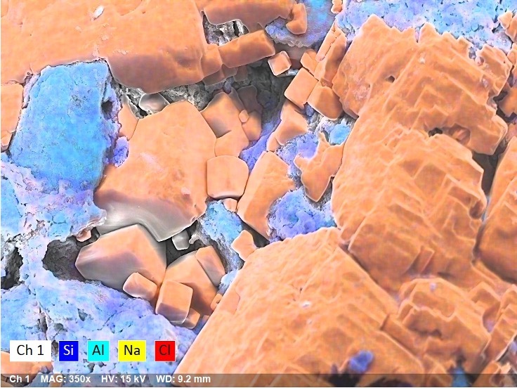
The need to examine a material or surface for features, particle size and shape, bumps, cracks or damage, or deeper information such as surface topography or roughness, grain size, or inhomogeneous phases is a common event in fields like materials science, geology, metallurgy, biology, forensics, and many other technical fields. For many larger or macro surfaces, optical microscopy is sufficient and a useful tool. But for cases where the features are smaller than can be resolved by typical light microscopy, scanning electron microscopy (SEM) is a powerful alternative.
SEM
Scanning Electron Microscopy (SEM) is a high-resolution microscopy technique that provides far greater magnification than optical or light microscopes. As opposed to conventional microscopy using light, SEM interrogates your material or sample of interest by rastering a beam of electrons across the surface and utilizes the interaction of the electrons with those of your material and creates images by collecting the secondary or backscattered electrons location by location. In this manner, SEM provides a much higher magnification than capable with light microscopy and can provide details of the sample surface and topography for features a few nanometers in size.
EDS
Besides the impressive imaging ability of the SEM, there are other useful analyses that can be performed in the SEM. As the electrons interact with the material and secondary electrons are ejected, the ionized atoms return to the ground state by dropping an electron down from the outer shell to fill the vacancy, and in this process an x-ray photon is released. This is a characteristic x-ray with a specific energy related to the atom and the transition and therefore when collected with a detector in the SEM can reveal elemental information. By doing this operation with the rastering beam and detecting from each spot, elemental maps for a spot, region, phase, or line across the sample can be generated. This is a very powerful way of in situ identifying phases or contaminants of interest or for ensuring the location of a specific portion of a sample such as a core, layer, or coating.
H&M SEM Capabilities
While many scientists and industries have or can access the older style tungsten filament type of SEM, outside of universities, accessing the newer and more powerful field emission SEM (FESEM) instruments is less common. The improvements to the beam brightness (intensity), focusing, electronics, et al. features make the imaging from these new scopes much brighter, sharper, and improved. H&M has a university level FESEM (Zeiss Gemini FE-SEM with Bruker XFlash 7 EDS spectrometer) and experienced staff capable of truly world class SEM imaging and analyses. Some examples of interesting images and projects are shown below.
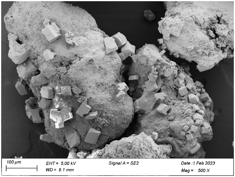
Figure 2 – High resolution image of a granular sample showing a cubic crystal growth on the surface. EDS maps show these cubes to be comprised of Na and Cl allowing us to positively identify them as Halite.
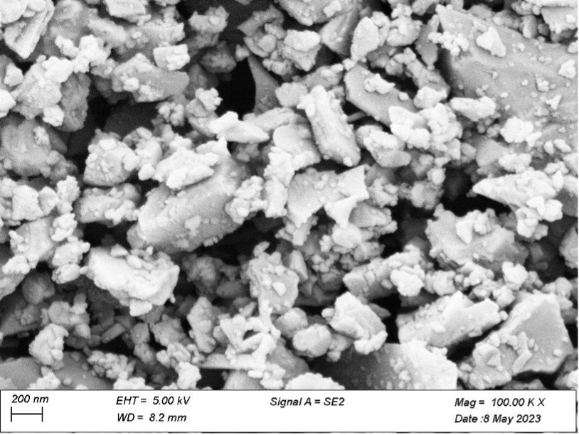
Figure 3 – High magnification (100,000x) imaging of a fine powder showing particle sizes in the 100-500nm range.
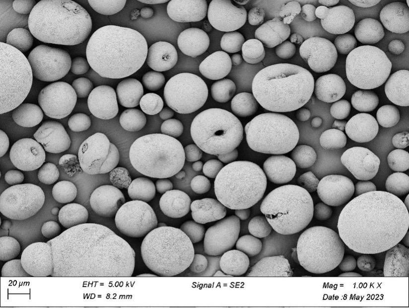
Figure 4 – High resolution image of a powder, showing spherical particles in the 20-100μm range.
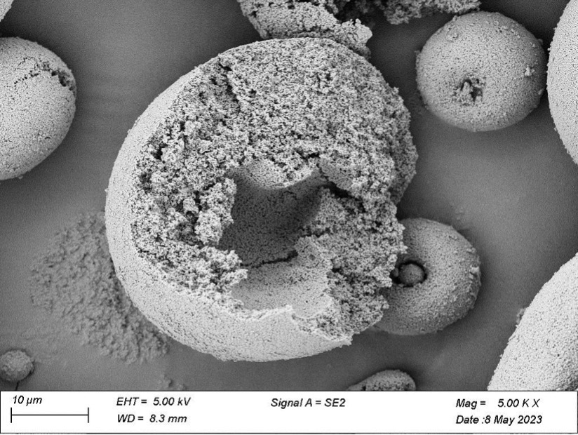
Figure 5 – Higher magnification image of the spherical powder shown in Figure 3, showing the surface texture and detail of a broken sphere and the general size of the smaller particles that compose the sphere.
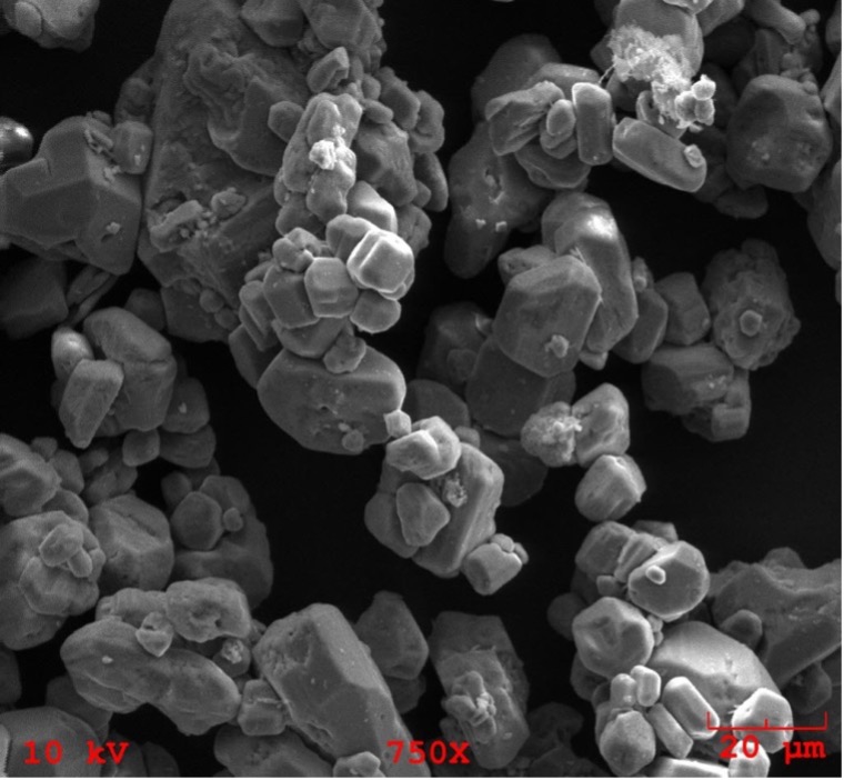
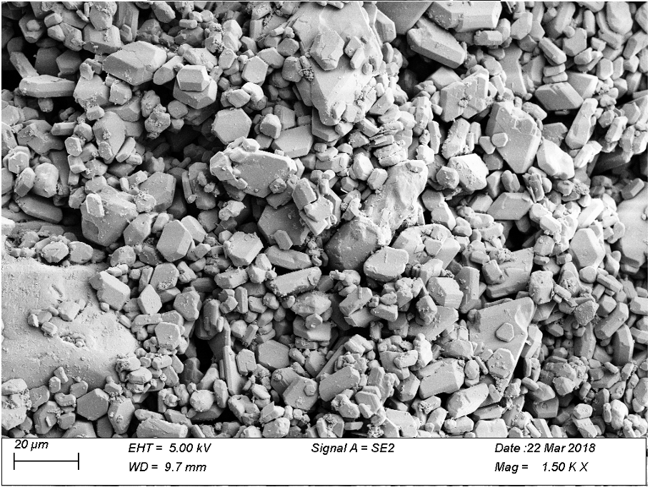
Figure 6 – Resolution and brightness comparison of a tungsten filament SEM (left) to the FE-SEM (right) both taken of samples of gypsum.

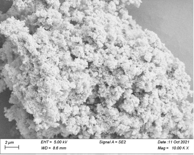
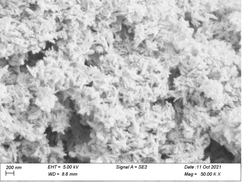
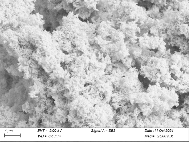
Figure 7 – Resolution comparison of a tungsten filament SEM (top left) at its highest resolution for this material, and significantly higher magnifications of the same type of sample using the FE-SEM, demonstrating the superior resolution capabilities of the FE-SEM.