
Scanning Electron Microscopy
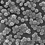
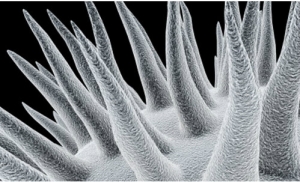
Scanning electron microscopy (SEM) is an analytical tool which can provide high resolution images of samples with a high depth of field. SEM is also extremely good at producing detailed images of surface topography. We utilize a Field Emission Scanning Electron Microscope (FESEM) to obtain the highest resolution possible with high brightness, providing the best images possible.
Our FESEM is equipped with an energy dispersive X-ray spectrometer (EDS) to provide composition information. This is an extremely useful characterization method for failure analysis, particle identification and reverse engineering purposes. They are also able to provide elemental mapping and utilize back scattered and secondary electron imaging to provide even more information on the sample.
Main Applications of Scanning Electron Microscopy
- Particle identification and characterization – shape, size, morphology
- Characterization of minerals and ores
- Elemental mapping and analysis
- Process characterization
- Dimensional analysis
- Device for component failure analysis
- Reverse engineering
- Forensic analysis
Detailed Analysis
The SEM is a powerful tool that enables for quick imaging and some chemical composition. This has use in many different areas such as failure analysis, detection of multi-layers of different compositions and more. An example of this is an unknown material with a range of particles of different compositions. The image taken by the SEM shows many particles of different sizes and shapes, but the composition of these particles needs to be identified. Utilizing the EDS attachment on the SEM allows H&M to map out the chemical components.
EDS can perform line scans across each of the individual particles. Once completed, the software will determine the chemical components that are in each of the scans. Since all of the detectors are linked together, the original SEM image can be transformed into an elemental map for ease of viewing. The figure below shows the completed elemental mapping with each color corresponding to a different composition.

Failure analysis of materials is a common practice in both industry and research and development. A practical first step is to observe the material in a SEM to get a good up close look at the issue. At that point, a closer examination of the particles and grains can lend itself to possible reasons for the failure. Knowing the composition and desired particle size distributions of the failed section can provide even more data. If the particles are too large, it could mean that the material in question did not undergo the required chemical reaction during production, thus leading to additional unwanted stress or strain in the material. The advantage of observing the material under SEM is that visual evidence of particle size, shapes and interactions can be found.
Technical Specifications of Equipment
- Signals Detected: Secondary and backscattered electrons and x-rays
- Elements detected: Boron to Uranium
- Detection Limits: ~1%
- Imaging/Mapping: Yes
- EDS Mapping Resolution: ~1 μm
- Image Resolution: 1.5 nm @ 30kV
Key Markets Served
- Pharmaceuticals
- Semiconductors
- Coatings and Adhesives
- Electronics
- Mining and Metals
- Aerospace
- Solar and Lighting
- Defense
- Data Storage
- Personal Care
- Packaging
- Life Sciences
- Law and Litigation